
Cover Story in Nano Letters: A Dot Projector Shrunk to a Chip
- Yao-Wei Huang

- Jul 24, 2025
- 2 min read
Updated: Sep 2, 2025
Our research has been spotlighted on the cover of Nano Letters, Volume 25, Issue 29, dated July 23, 2025.
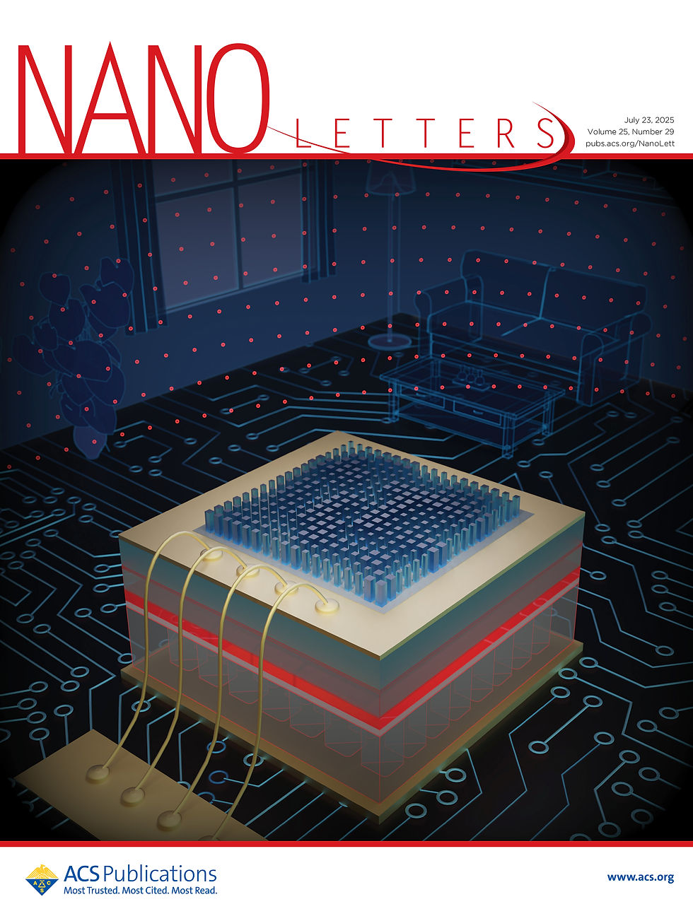
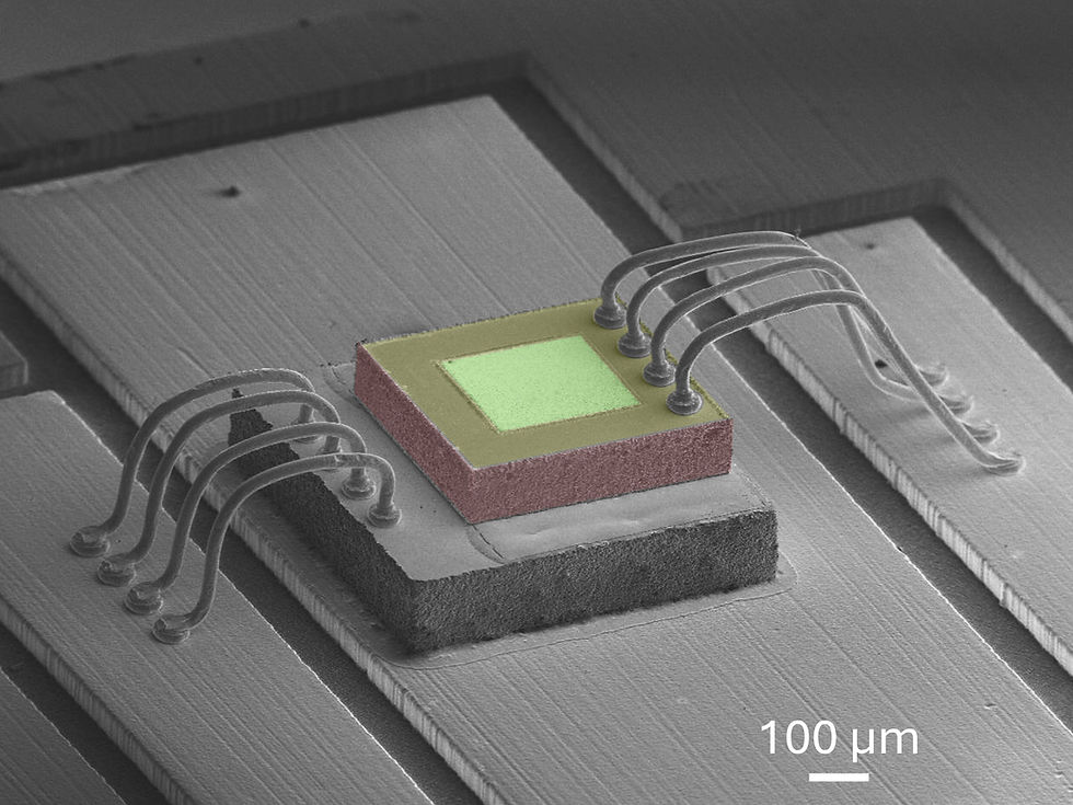
About the Cover: A monolithic metasurface-PCSEL chip enables chip-scale dot projection. It achieves an ultracompact 0.025 mm³ footprint and 28.7% lower power, it is over 2400× smaller, and is more efficient than commercial systems. Structured-light projections support smartphones, extended reality, and biometrics. A virtual scene emerges from the projected dots, symbolizing next-generation depth sensing on chip.
關於封面:單晶整合超穎介面-PCSEL 晶片,實現了晶片級的點陣投影儀。其體積僅有 0.025 mm³,比商用系統小超過 2400 倍。效率也更高,功耗降低 28.7%。其結構光投影可支援智慧型手機、延展實境與生物辨識等應用。投影出的點陣構築出虛擬場景,象徵著下一世代晶片上深度感知技術的來臨。
Abstract: We demonstrate the first monolithic integration of a metasurface hologram and a photonic crystal surface-emitting laser (PCSEL) to realize a chip-scale structured light projector. This approach achieves unprecedented reductions in both device footprint and power usage, while preserving practical 3D sensing capabilities. Our wafer-level design features a compact footprint of 0.025 mm³, representing an approximately 2450-fold reduction in volume compared to commercial DOE-VCSEL dot projectors, while also reducing power consumption by 28.7%. The integration strategy offers promising fabrication compatibility and represents a transformative advancement in a compact transceiver system, paving the way for next-generation applications in biometrics, extended reality, and consumer electronics.
摘要:本研究首次實現超穎介面全像片與光子晶體面射型雷射的單晶整合,開發出晶片級結構光投影儀。此方法在大幅縮小元件體積與降低功耗的同時,仍保有實用的三維感測能力。我們的晶圓級設計具有 0.025 mm³ 的超小尺寸,相較於商用 DOE-VCSEL 點投影器,其體積縮小約 2450 倍,功耗也降低了 28.7%。此整合策略具備優異的製程相容性,為小型化光電收發系統帶來重大突破,為次世代生物辨識、延展實境及消費性電子產品等應用開啟嶄新契機。


Comments